In today's well-networked, modern and digital world, smartphones, autonomous vehicles, AI infrastructure and even in space research and defense are the basis of almost all innovations. They take part and are now the backbone of modern digital economies.
Since the worldwide demand for computing power escalates, the nations and industry focus on ensuring a stable, high-quality, scalable semiconductor supply chain. In view of the demand, the need for innovation in manufacturing processes becomes increasingly critical and shortens the time for market and costs. Engineering simulations are continued as a key lever to increase productivity and be due to the value chain of the Semiconductor production.
Semiconductor market
The semiconductor industry recorded 19% growth in 2024 and achieved $ 627 billion with forecasts of $ 697 billion this year. It is on the right track for the turnover of 1 trillion US dollar by 2030 and may reach 2 trillion US dollars by 2040, driven by 5G, AI, IoT and electromobility. Disruptions of the supply chain and increasing design complexity accelerate investments in domestic chip production in different regions. The USA, Europe, Taiwan, Korea and China have all announced significant incentives to support FABS and CHIP design. India also has many initiatives for the construction of factories, OSAT facilities and an indigenous ecosystem. The government has initiated the India Semiconductor Mission or ISM with an incentive of 10 billion US dollars to create global and local investments in the production of chips, the design, the exhibition and F&E.
Why concentrate on the production of semiconductors?
Although India has a solid electronics market, the nation is heavily dependent on imports for key components. Production is the most capital-intensive stage in the Semiconductor value chain. Every step from cleaning the raw silicide cleaning to the production and packaging of Wafer must meet benchmarks, including strict yield, purity and performance. Technical options during the design, validation and scaling levels directly influence the chip production economy.
Successful production of semiconductors requires a massive scale, precision technology and relentless innovation. Extended tools are also required that reduce the presumption, cut prototype cycles and simulate real physics before a product hits the line.
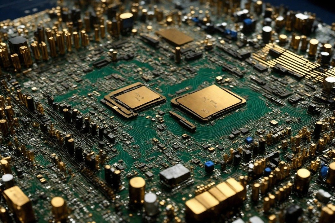
Semiconductor manufacturing process and technical challenges in the entire value chain
The semiconductor value chain is complicated and comprises several stages.
- The production of the semiconductors includes oxidation, etching, doping, deposition and photolithography.
- Blind -wafer production, including silicon crystal growth, cutting, designing, shopping and polishing.
- Assembly and packaging that cover the integration of preparation, binding, molded parts and print sheath (print).
- Tests & Inspection evaluates the chip performance under various environmental and usage scenarios.
Each of the above phases has its own challenges:
- Wafer production includes hundreds of steps such as photolithography, etching and storage on the nanometer scale. Even microscopic variances can influence the performance or lead to loss of earnings.
- Packaging and tests require the balancing size, thermal dissipation, performance and signal integrity.
- Time for market, cost pressure, return optimization and reliability are constant concerns. The most important aspects include reducing design cycles, the acceleration of system validation and the decision of front load processes.
- Earnings optimization: The control of wafer pollution, the uniform film deposit and the variability of the management of the processes is essential.
- Cost control: reduction in prototype editions, test cycles and equipment rework. Is key
A quick miniaturization and the advance towards 2NM and 3D chip architectures deepen these challenges. A single error in the uniformity of the deposition or thermal control can derail the yield and influence reliability. Traditional methods are impossible because they often rely on experiments and errors and are reactive, which makes it inadequate for today's nanoscale complexities.
Simulation is a player for the production of semiconductors
If devices are smaller, faster and more powerful, the complexity of the production is only deepened. The integration of AI in simulation, high-performance computing and digital twins will revolutionize semiconductor research and development and production. The simulation will therefore be of crucial importance for the optimization of existing processes and to enable innovations in heterogeneous integration, 3D packaging and sustainable FAB operations.
Simulation enables engineers to practically prototypes every aspect of the Semiconductor manufacturing process. These tools offer implementable insights into the process performance, the failure risks and system behavior by integrating fluid dynamics, structural mechanics, electromagnetics and material science.
Here are some important simulation applications in the value chain:
- Polysilicium production and crystal growth: simulation increases reactor heating and gas flow for even rod growth. This cut prototyping requires and improves the Ingot yield.
- Wafer handling processes such as zipper and zipper must be simulated exactly to ensure reliable and error -free manipulation of sensitive wafers. In addition, understanding the effects of these processes on wafer distortion is of crucial importance for the optimization of the handling parameters and to improve the overall output.
- Wafer cubes are a critical process that has a direct effect on the yield and general device reliability. In order to maximize the yield, it is important to optimize the process parameters. The standard techniques include SAW cubes and laser cubes, depending on the use unique advantages. In view of the brittle nature of Wafern and the presence of sensitive shifts, the reaching of clean and precise cuts is of crucial importance. Thorough validation and tests are required, and the simulation plays a key role in understanding and improving the cube process.
- The preparation and cleaning of the cubes: CFD models improve the wet cleaning efficiency, the loss design and the particle removal. This leads to faster cycle times and improved cleanliness.
- Heat processes (e.g. heat treatment, ALD, PECVD): Simulations guarantee temperature equality, reduce stress -induced defects and help with the deposit rates of fine -tuning.
- Chemical mechanical polishing (CMP): High-fidelity models optimize the contact conditions for the upswing and pad pad contact in order to reduce better abrasion performance and reducing material waste.
- Lithography & etching: Optical and chemical simulations increase mask resolution, predictions of etching profiles and reduce the iterations of the board, which accelerates ramp-to-production.
- Assembly and packaging: From the Lötin -Reflow modeling to the get -the -thing forecast and the Moldflow simulation, the simulation ensures reliable chip packs under thermal and mechanical tension.
- Simulations are becoming increasingly important for the design and optimization of advanced ICs such as 3Dics. They help engineers, mechanical stress, thermal distribution and electrical performance to analyze over stacked layers that are more pronounced in these complex constructions. Simulating the material behavior and the connection performance accelerates the development process and improves the total output of 3D ICS.
All of this also leads to some measured business effects. The system validation time is shortened by 66%. An improvement of up to 90% can be observed under operating conditions for a better return, and there will also be up to 10 times the savings in energy consumption via optimized process controls.
Simulation can help manufacturers to switch from a “build and test” approach to a “simulate and optimize”. This saves both time and money and improves product quality and consistency.
Future prospect
Engineering simulations create a massive value for chip makers in this rapidly developing market by approaching returns, time and costs. Simulation-managed engineering is a player in the developing semiconductor ecosystem of India. Simulation-driven productivity and earnings improvements are of crucial importance for manufacturers in order to be competitive worldwide.
If India builds up its semiconductor in the future, taking simulation will help to overcome barriers. Simulation is not only a support tool, but of crucial importance for the success of the semiconductor.
Disclaimer: This is an article written by guest. Opinions and information is solely that of the author. The machine manufacturer does not guarantee the accuracy of the content and assumes no liability for statements or claims contained therein.